Metal with ohmic contact on n-type Silicon
a) The electron affinity of Si is 4.05 eV, the work functions of Al, W and Au are 4.4, 4.6 and 5.1 eV. What metal would for ohmic contact on an n-type Si, and on a p-type Si?
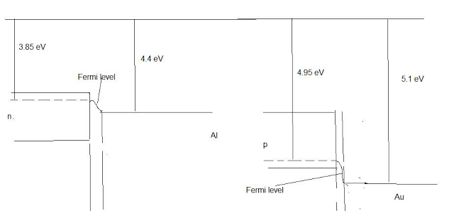
b) Draw schematically the band diagram for the two above cases, assuming a dopant concentration $10^{18} cm^{-3}$ .
c) Estimate the build-in voltage and depletion region width.
Answer
The Gap Band of Si is $E_g =1.11 eV$
The donor or acceptor level can be approximated to be pinned about at the conduction (respectively valence band) The difference in energies is less than $0.1 eV$.
Thus for $n$ type the work function of Si (difference between donor level – Fermi level and vacuum level) is $4.4-(1.1/2) =3.85 eV$
The closest material for a ohmic contact is Al ($4.4 eV$ work function)
For $p$ type the work function is $4.4+(1.1/2) =4.95 eV$.
The closest material for a ohmic contact is Au.
b) The donor or acceptor level position does not depend on the dopant concentration. It depends on the type of dopant. It is always about $0.1 eV$ energy difference from the corresponding band. The figures are below.
c) The build in voltage for n type is $V_b=4.4-3.85 =0.55 V$
the build in voltage for the $p$ type is $V_b=4.95-5.1 =-0.15 V$
The width $W = W_1+W_2$ of the depletion region is estimated from
$W =sqrt{(2*epsilon / e)*(1/N)*V_b}$
where $N$ is given $N=10^{18} cm^{-3} =10^{24} m^{-3}$
and $epsilon=11.7*epsilon_0 =11.7*8.854*10^{-12} =10^{-10} F/m$
$W =sqrt {(2*10^{-10}/1.6*10^{-19})*1/10^{24} *0.55}=26.2 nm$ for $n$ type
$W = sqrt {(2*10^{-10}/1.6*10^{-19})*1/10^{24} *0.15} =13.7 nm$ for $p$ type

